- 您现在的位置:买卖IC网 > Sheet目录3827 > PIC16F877A-I/P (Microchip Technology)IC MCU FLASH 8KX14 EE 40DIP
2003 Microchip Technology Inc.
DS39582B-page 157
PIC16F87XA
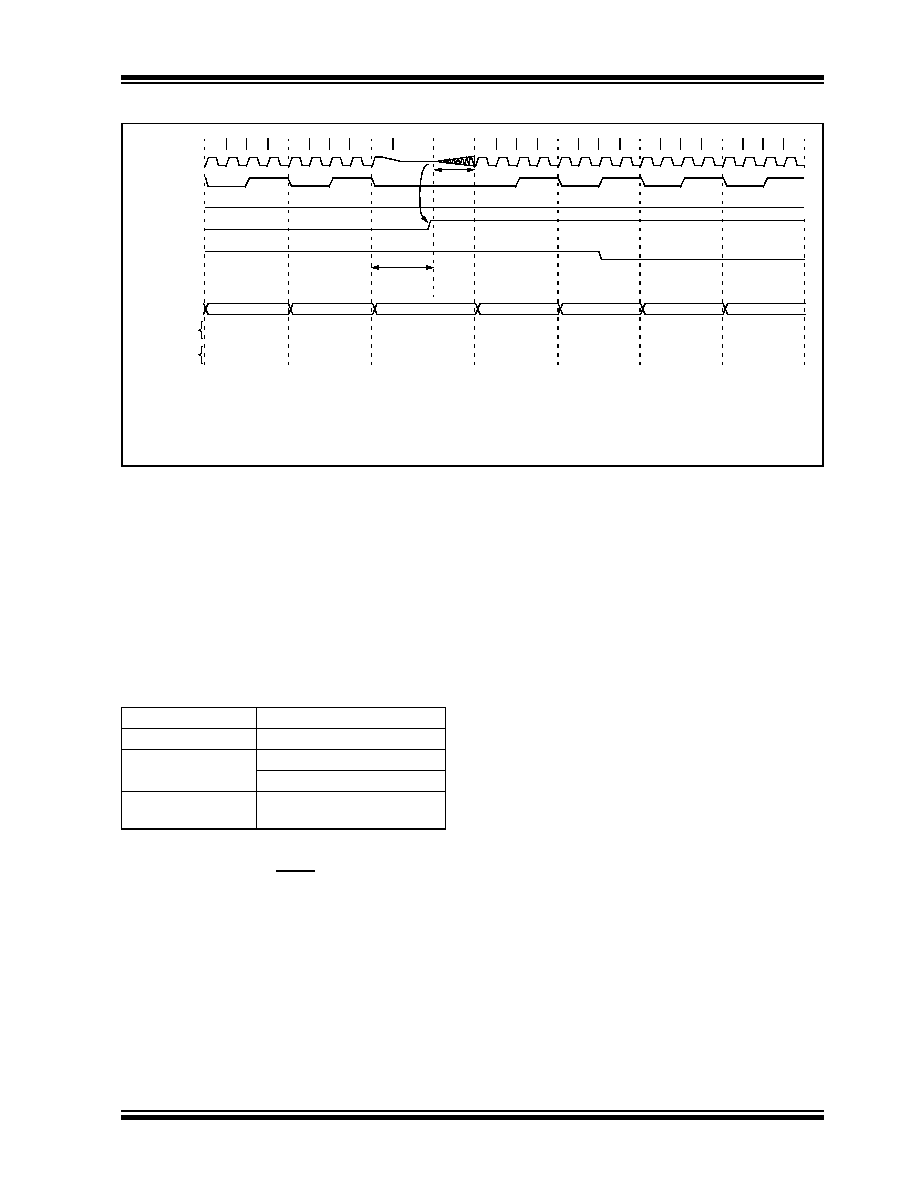
FIGURE 14-12:
WAKE-UP FROM SLEEP THROUGH INTERRUPT
14.15 In-Circuit Debugger
When the DEBUG bit in the configuration word is pro-
grammed to a ‘0’, the in-circuit debugger functionality is
enabled. This function allows simple debugging
functions when used with MPLAB ICD. When the
microcontroller has this feature enabled, some of the
resources are not available for general use. Table 14-8
shows
which
features
are
consumed
by
the
background debugger.
TABLE 14-8:
DEBUGGER RESOURCES
To use the in-circuit debugger function of the microcon-
troller, the design must implement In-Circuit Serial Pro-
gramming connections to MCLR/VPP, VDD, GND, RB7
and RB6. This will interface to the in-circuit debugger
module available from Microchip or one of the third
party development tool companies.
14.16 Program Verification/Code
Protection
If
the
code
protection
bit(s)
have
not
been
programmed, the on-chip program memory can be
read out for verification purposes.
14.17 ID Locations
Four memory locations (2000h-2003h) are designated
as ID locations, where the user can store checksum or
other code identification numbers. These locations are
not accessible during normal execution but are
readable and writable during program/verify. It is
recommended that only the 4 Least Significant bits of
the ID location are used.
Q1 Q2 Q3 Q4 Q1 Q2 Q3 Q4 Q1
Q1 Q2 Q3 Q4 Q1 Q2 Q3 Q4 Q1 Q2 Q3 Q4 Q1 Q2 Q3 Q4
OSC1
CLKO(4)
INT pin
INTF Flag
(INTCON<1>)
GIE bit
(INTCON<7>)
INSTRUCTION FLOW
PC
Instruction
Fetched
Instruction
Executed
PC
PC+1
PC+2
Inst(PC) = Sleep
Inst(PC - 1)
Inst(PC + 1)
Sleep
Processor in
Sleep
Interrupt Latency(2)
Inst(PC + 2)
Inst(PC + 1)
Inst(0004h)
Inst(0005h)
Inst(0004h)
Dummy cycle
PC + 2
0004h
0005h
Dummy cycle
TOST(2)
PC+2
Note 1: XT, HS or LP Oscillator mode assumed.
2: TOST = 1024 TOSC (drawing not to scale). This delay will not be there for RC Oscillator mode.
3: GIE = 1 assumed. In this case, after wake- up, the processor jumps to the interrupt routine.
If GIE = 0, execution will continue in-line.
4: CLKO is not available in these oscillator modes but shown here for timing reference.
I/O pins
RB6, RB7
Stack
1 level
Program Memory
Address 0000h must be NOP
Last 100h words
Data Memory
0x070 (0x0F0, 0x170, 0x1F0)
0x1EB-0x1EF
发布紧急采购,3分钟左右您将得到回复。
相关PDF资料
MP2-HS240-51
CONN SHROUD 2-FB 240POS 5ROW
DSPIC33FJ64MC506-I/PT
IC DSPIC MCU/DSP 64K 64TQFP
DSPIC33FJ128MC802-I/SO
IC DSPIC MCU/DSP 128K 28SOIC
PIC18LF4331-I/P
IC PIC MCU FLASH 4KX16 40DIP
DSPIC33FJ128GP306-I/PT
IC DSPIC MCU/DSP 128K 64TQFP
PIC24HJ128GP306-I/PT
IC PIC MCU FLASH 128KB 64TQFP
PIC16F873-20/SO
IC MCU FLASH 4KX14 EE 28SOIC
PIC18F4431-I/P
IC PIC MCU FLASH 8KX16 40DIP
相关代理商/技术参数
PIC16F877A-I/P
制造商:Microchip Technology Inc 功能描述:IC 8BIT FLASH MCU 16F877 DIP40
PIC16F877A-I/PG
功能描述:8位微控制器 -MCU 14KB 368 RAM 33 I/O RoHS:否 制造商:Silicon Labs 核心:8051 处理器系列:C8051F39x 数据总线宽度:8 bit 最大时钟频率:50 MHz 程序存储器大小:16 KB 数据 RAM 大小:1 KB 片上 ADC:Yes 工作电源电压:1.8 V to 3.6 V 工作温度范围:- 40 C to + 105 C 封装 / 箱体:QFN-20 安装风格:SMD/SMT
PIC16F877A-I/PT
功能描述:8位微控制器 -MCU 14KB 368 RAM 33 I/O RoHS:否 制造商:Silicon Labs 核心:8051 处理器系列:C8051F39x 数据总线宽度:8 bit 最大时钟频率:50 MHz 程序存储器大小:16 KB 数据 RAM 大小:1 KB 片上 ADC:Yes 工作电源电压:1.8 V to 3.6 V 工作温度范围:- 40 C to + 105 C 封装 / 箱体:QFN-20 安装风格:SMD/SMT
PIC16F877A-I/PT
制造商:Microchip Technology Inc 功能描述:8BIT FLASH MCU SMD 16F877 TQFP44
PIC16F877A-I/PTG
功能描述:8位微控制器 -MCU 14KB 368 RAM 33 I/O RoHS:否 制造商:Silicon Labs 核心:8051 处理器系列:C8051F39x 数据总线宽度:8 bit 最大时钟频率:50 MHz 程序存储器大小:16 KB 数据 RAM 大小:1 KB 片上 ADC:Yes 工作电源电压:1.8 V to 3.6 V 工作温度范围:- 40 C to + 105 C 封装 / 箱体:QFN-20 安装风格:SMD/SMT
PIC16F877AIL
制造商:Microchip Technology Inc 功能描述:
PIC16F877AIP
制造商:Microchip Technology Inc 功能描述:
PIC16F877AIPT
制造商:Microchip Technology Inc 功能描述: